https://doi.org/10.1038/s41598-020-59854-y
“The absence of centrosymmetry in chiral and polar crystal structures is the reason for many technical relevant physical properties like optical birefringence or ferroelectricity. Other chirality related properties that are actually intensively investigated are unconventional superconductivity or unusual magnetic ordering like skyrmions in materials with B20 structure. Despite the often close crystal structure – property relation, its detection is often challenging due to superposition of domains with different absolute structure e.g. chirality. Our investigations of high quality CoSi crystals with B20 structure by both complementary methods X– ray (volume sensitive) and electron backscatter diffraction (EBSD) (surface sensitive) results the consistent assignment of the chirality and reveal fundamental differences in their sensitivity to chirality. The analysis of the surface of a CoSi crystal with domains of different chirality show the high spatial resolution of this method which opens the possibility to analyze the chirality in microstructures of technical relevant materials like thin films and catalysts.”
”
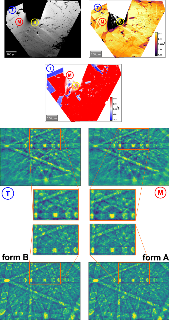
In combination with the calibration of the absolute structure that was achieved by the X-ray characterization, the excellent spatial resolution provided by the EBSD method allows to characterize the local chirality of multi-domain crystals. Figure 4 shows EBSD mapping and chirality assignment of domains of a CoSi crystallite. This sample was prepared by chemical vapor transport process as well. The EBSD measurements are performed on the as-grown surface of the crystal without further metallographic preparation. The backscattered electron (BSE) image of the sample is shown in Fig. 4 (top left) (Supplementary, Fig. S1: light optical image). The EBSD measurements were carried out in a polygonal masked part of the total map area of 400 × 300 points at a step size of 3.8 µm. The region marked by ‘S’ is shadowed by another crystal outside of the masked area (Fig. 4 top). The experimental Kikuchi pattern shown in Fig. 4 (middle) are measured in the regions ‘M’ and ‘T’ with a resolution of 320 × 228 pixels. The slowly varying background part in the raw Kikuchi patterns has been removed by high-pass filtering to emphasize the diffraction signal. In order to allow a direct comparison with simulated Kikuchi patterns of the A form and B form (Fig. 4 bottom), all patterns have been normalized to zero mean and unit standard deviation. The values of the average cross correlation rm = 0.64–0.68 (Fig. 4 top right) reflect the high quality of the experimental pattern and the very good agreement with the simulations in almost the whole masked area with exception of area ‘S’ with values rm <0.52 due to shadowing. Values of the cross correlation differences are in the range ∆r = +/−0.02. The mapping of ∆r in Fig. 4 (top, second row) visualize that the main part is characterized by ∆r ≈ +0.02 e.g. the A form is realized in these areas. In smaller regions with ∆r ≈ −0.02 the inverted crystal structure is present. In most of the masked area these ∆r values are sufficiently high to distinguish between both absolute structures. In the shadowed area ‘S’ the small values rm does not allow a reliable assignment of the absolute structure by the cross correlation values.
Surface of a CoSi crystallite showing domains of different chirality; (top left) SEM image (SE contrast; 70° tilt corrected; s.a. Supplementary Figure S1); (top right) mean value rm=(r+E+r−E)2��=(�+�+�−�)2; of cross correlation coefficients r+E,r−E that quantify the coincidence between images of measured EBSD pattern and simulated pattern of both enantiomorphs, (second row) cross correlation coefficient difference (Δr=r+E−r−EΔ�=�+�−�−�), red regions result from better coincidence with EBSD pattern of the A form, blue regions result from better coincidence with EBSD pattern of the B form of the CoSi crystal structure, (middle) measured EBSD patterns from region “T” and “M” with magnified details below, (bottom) simulated EBSD patterns of the A and B form of the CoSi crystal structure with enlarged details above. The detail images (orange frames) visualize the high coincidence between measured and simulated pattern as well as chirality dependent differences in intensity and shape of local spots (see for example upper left corner with localized and broadened spots).
“

